
solder mask applied in Electronic assembly near me
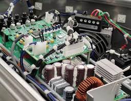
In electronic assembly, the application of solder mask is a critical step in ensuring the reliability and performance of printed circuit boards (PCBs). Whether you’re seeking electronic assembly services nearby or managing assembly processes in-house, understanding how solder mask is applied is essential for producing high-quality PCBs. Solder mask, also known as solder resist, is a protective layer applied to the surface of PCBs to insulate conductive traces and prevent unintended solder bridges during assembly.
The process of applying solder mask typically begins after the PCB has undergone various fabrication steps, including etching, drilling, and copper plating. Once the bare copper traces and pads are exposed, the PCB enters the solder mask application stage. There are several methods for applying solder mask, with the most common being liquid photoimageable (LPI) solder mask and dry film solder mask.
In the liquid photoimageable solder mask process, a liquid solder mask material is applied to the surface of the PCB using various methods such as screen printing, spray coating, or curtain coating. The solder mask is then dried to remove excess solvent, leaving a thin, uniform layer of solder mask material covering the electronic assembly near me surface. Next, the solder mask is exposed to ultraviolet (UV) light through a phototool or mask, which contains the desired pattern of openings for solder mask removal. The UV light cures the solder mask material in areas not covered by the mask, creating a hardened protective layer over the copper traces and pads.
How is solder mask applied in Electronic assembly near me?
After exposure to UV light, the PCB undergoes a development process where the uncured solder mask material is removed using a developer solution. This solution washes away the unexposed solder mask material, leaving behind the cured solder mask in the desired pattern defined by the phototool. The PCB is then subjected to a final curing process, typically through heat exposure, to further harden the solder mask and enhance its durability.
Alternatively, dry film solder mask can be applied to the PCB using a similar process to dry film photoresist. A pre-cut sheet of solder mask material is aligned and laminated onto the PCB surface using heat and pressure, ensuring intimate contact between the solder mask film and the PCB substrate. The PCB with the solder mask film is then exposed to UV light through a phototool, followed by a development process to remove the uncured solder mask material. Finally, the PCB undergoes a curing process to fully harden the solder mask film and enhance its adhesion to the PCB surface.
Regardless of the method used, the application of solder mask is a critical step in electronic assembly that directly impacts the reliability and performance of PCBs. Properly applied solder mask provides insulation and protection to the underlying copper traces and pads, reducing the risk of short circuits, corrosion, and other electrical issues. By understanding the solder mask application process, manufacturers can ensure the quality and integrity of PCBs in electronic assemblies, ultimately delivering reliable products to customers.


