PCB Design Assembly
The evolution of assembled printed circuit boards (PCBs) has fueled the performance capabilities of electronic devices, from smartphones to aerospace applications. From improved manufacturing techniques to the use of cutting-edge materials, these advancements contribute to a comprehensive transformation in how PCBs are designed and manufactured.
One notable trend in this landscape is the integration of automation into the pcb design assembly process, which enables streamlined workflows and minimizes human error to ensure high-quality outcomes. Other key innovations include the use of intelligent software systems to monitor real-time data for optimization and the implementation of eco-friendly materials to align with sustainability goals.
As the demand for electronic devices continues to grow, PCBs are becoming increasingly compact and power-efficient. The use of HDI technology is contributing to this trend by allowing more components to be packed into smaller spaces. This is achieved through the use of microvias, blind and buried vias, and fine lines and spaces to deliver higher wiring density, making HDI PCBs ideal for mobile phones and other compact devices.
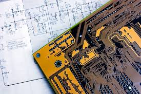
Advancements in PCB Design Assembly
Other innovations in PCB design and assembly are enabling higher speeds and better signal transmission by using special designs and materials that reduce signal interference and loss. This is particularly important in high-speed data transfer and RF applications, which requires PCBs to be able to operate at high frequencies and speeds.
Additionally, the incorporation of 3D printing into PCB fabrication allows for more complex geometries to be produced that would be difficult or impossible to produce with traditional methods. This allows for a more customized design that better matches the requirements of specific electronics products, while also increasing flexibility and speeding up the prototyping process.
When it comes to assembling the components onto the PCB, advanced technologies like automated soldering and inspection systems help manufacturers streamline production processes and ensure quality results. These tools use automated vision systems to precisely position surface mount components, minimizing errors and reducing rework costs. Additionally, X-ray inspection can examine through-hole components to detect hidden defects, including voids or insufficient solder, which may lead to poor electrical connections.
Once all the components are in place, the board is passed through a reflow oven where molten solder flows over the exposed metal areas and component leads to create strong and reliable joints. This step may also be augmented with functional testing to verify that the complete device operates as intended under real-world conditions.
Another area of ongoing innovation in assembled PCBs is the development of new materials that enhance performance, reliability, and versatility. For example, the introduction of advanced substrates with unique properties, such as low thermal expansion and good mechanical stability, can enable designers to produce lighter, thinner, and more compact PCBs. Similarly, the development of conductive inks that can be applied directly to a substrate has opened up the possibility for innovative new products, such as flexible PCBs. This type of PCB is ideal for devices that need to be able to bend or twist without breaking, such as medical and military equipment.