
materials are used in the fabrication of HDI PCBs
The fabrication of High-Density Interconnect (HDI) printed circuit boards (PCBs) requires the use of specialized materials that can meet the stringent requirements of high-density, high-performance electronic applications. These materials play a crucial role in ensuring the reliability, functionality, and durability of HDI PCBs across various industries.
One of the primary materials used in the fabrication of HDI PCBs is the substrate material, which serves as the foundation for the circuitry. Common substrate materials include epoxy-based laminates such as FR-4 (Flame Retardant 4) and FR-4 High Tg (High Glass Transition Temperature), as well as polyimide-based laminates such as Kapton. These materials offer excellent electrical insulation properties, mechanical strength, and thermal stability, making them suitable for use in a wide range of electronic applications.
Moreover, the choice of copper foil is critical in hdi pcb fabrication, as it forms the conductive pathways that carry electrical signals between components and layers. Copper foils are available in various thicknesses and surface finishes, depending on the specific requirements of the application. Thinner copper foils are often used in HDI PCBs to enable finer trace widths and tighter routing configurations, while surface finishes such as ENIG (Electroless Nickel Immersion Gold) or OSP (Organic Solderability Preservatives) enhance solderability and protect against oxidation.
What types of materials are used in the fabrication of HDI PCBs?
Furthermore, the fabrication of HDI PCBs may involve the use of advanced materials such as high-performance laminates and thin copper foils. High-performance laminates offer superior electrical properties, including low dielectric constant and loss tangent, as well as excellent thermal conductivity and stability. These materials are particularly well-suited for high-frequency applications where signal integrity and impedance control are critical.
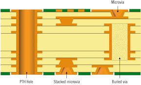
In addition to substrate and copper foil materials, the fabrication of HDI PCBs may also involve the use of specialized materials for vias and microvias. Vias are conductive pathways that connect different layers of the PCB, while microvias are smaller vias used in HDI PCBs to achieve higher circuit densities. These vias and microvias are typically filled with conductive materials such as copper or conductive epoxy to ensure reliable electrical connections between layers.
Moreover, solder mask materials are used to protect the copper traces and vias on the surface of the PCB from environmental factors such as moisture, dust, and contaminants. Solder mask materials are applied to the surface of the PCB using a silk-screening process and are then cured to form a protective layer. Additionally, solder mask materials are available in various colors to facilitate identification and assembly processes.
Furthermore, adhesives and bonding materials are used in HDI PCB fabrication to laminate multiple layers of circuitry together and to attach components to the substrate. These materials must provide strong adhesion, thermal stability, and chemical resistance to withstand the rigors of the manufacturing process and the operating conditions of the final electronic device.
In conclusion, the fabrication of High-Density Interconnect (HDI) printed circuit boards (PCBs) requires the use of specialized materials that can meet the stringent requirements of high-density, high-performance electronic applications. These materials include substrate materials, copper foils, high-performance laminates, vias and microvias, solder mask materials, adhesives, and bonding materials. By carefully selecting and utilizing these materials, manufacturers can produce HDI PCBs that offer exceptional reliability, functionality, and durability across various industries.


