
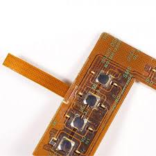
Reliability in FPC Circuit Boards
FPC (Flexible Printed Circuit) is a flexible substrate used to mount electrical components. The technology is especially useful for electronic products that require a flexible design, such as smartphones and other mobile devices. FPCs can be easily bent, wound and folded in three dimensions, which allows them to meet space layout requirements and reduce overall product weight and volume. They are also easier to inspect than rigid PCBs. The resulting benefits of flexible circuits include reduced assembly and shipping costs, faster time to market, and increased reliability.
The flexibility of FPCs makes them a viable alternative to traditional Rigid Circuit Boards (PCB) for a variety of applications. They are especially suited for consumer electronics, where the need to minimize size and weight is most critical. For example, the use of a fpc circuit board in a smartphone allows the manufacturer to reduce the amount of plastic required to house the phone.
While a FPC can be fabricated in many ways, one of the most common methods is transfer printing with conductive carbon ink. This method is relatively cheap and produces high quality circuitry. A wide range of shapes and thicknesses can be made using this technique, making it suitable for a wide variety of electronic products.
Solder Joint Reliability in FPC Circuit Boards
The mechanical performance of a FPC is largely determined by the bending reliability of its solder joints. Traditionally, 3-point and 4-point bending tests are used to determine the bending strength of FPCs. However, these tests are not accurate for assessing the bending reliability of FPCs with soft substrates. A new approach is needed to assess the bending reliability of FPCs with softer substrates.
A key factor in determining a solder joint’s reliability is its ability to withstand thermal shock. This is caused by sudden changes in temperature that cause the solder alloy to undergo microstructural changes. Typically, these changes occur in areas of high stress, such as at the corners and edges of the joint.
To prevent thermal shock, it is important to minimize the temperature gradient across a solder joint. This can be achieved by minimizing the difference between the component temperature and the board temperature, as well as ensuring that there is no mismatch in coeffcients of thermal expansion.
Besides thermal shock, another major reason for solder joint failure is corrosion. Corrosion is driven by electrochemical reactions that oxidize the solder and its nearby conductors. This can lead to a dark film on the exposed surface, and is often accompanied by an increase in resistance of the solder. Various factors can trigger these electrochemical reactions, including excess moisture and condensation, the presence of left over solder flux residues, and the chemical vapor deposition (CVD) process.
Finally, mechanical cycling and shock can lead to shear stress on solder joints, causing them to crack. This can be due to excessive deformation, such as a distorted housing, or from shear forces acting on the joints themselves. To determine the fatigue life of a solder joint, it is necessary to simulate the combined effects of thermal loading and mechanical loading. Using a multiphysics solver can help to examine the effects of both, allowing you to optimize your component placements and design for improved thermal and mechanical performance.


