
Assembly company pcb differ from PCB fabrication
When discussing electronic manufacturing, two terms often come up: PCB assembly and PCB fabrication. While they are related processes, they serve different functions in bringing electronic devices to life. Understanding the distinctions between PCB assembly and PCB fabrication is crucial for grasping the entirety of the manufacturing process.
PCB fabrication is the initial stage in the production of a printed circuit board (PCB). It involves the creation of the bare board, which serves as the foundation for the electronic components to be attached later in the assembly process. The fabrication process starts with the substrate material, usually a rigid laminate such as FR4, which provides the structural support for the circuit. Other materials, like polyimide or metal-core substrates, may be used for specific applications requiring flexibility or enhanced thermal conductivity.
The fabrication process continues with the application of a thin layer of copper to both sides of the substrate. This copper layer serves as the conductive pathways that connect the electronic components. A layer of photoresist is then applied to the copper surface, which is selectively exposed to UV light through a photomask. This exposure creates a pattern on the photoresist, defining where the copper will remain after the etching process.
How does Assembly company pcb differ from PCB fabrication?
Next, the assembly company pcb undergoes an etching process to remove the excess copper, leaving behind the desired circuit traces according to the pattern defined by the photoresist. Once the etching is complete, the remaining photoresist is stripped away, revealing the copper traces on the substrate. Holes are drilled or punched through the board at specific locations to accommodate through-hole components and facilitate interconnection between different layers of the PCB.
After the fabrication process, the bare PCB undergoes inspection to ensure that it meets quality standards and tolerances. Any defects or irregularities are addressed before the board proceeds to the assembly stage. PCB fabrication is primarily concerned with creating the physical substrate and copper traces that form the basis of the electronic circuit, without any components attached.
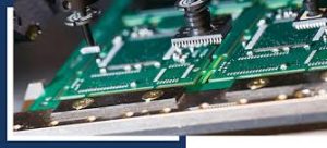
On the other hand, PCB assembly is the process of populating the bare PCB with electronic components to create a functional circuit. This involves soldering various components, such as resistors, capacitors, integrated circuits, and connectors, onto the PCB according to a predetermined layout or schematic diagram. PCB assembly can be divided into two main categories: surface mount technology (SMT) assembly and through-hole assembly.
In SMT assembly, components are mounted directly onto the surface of the PCB, eliminating the need for holes to pass through the board. This allows for denser component placement and smaller overall PCB size, making it suitable for compact and lightweight electronic devices. SMT components are typically soldered onto the board using reflow soldering techniques, where solder paste is applied to the board before components are placed and heated to melt the solder.
Through-hole assembly, on the other hand, involves mounting components with wire leads through pre-drilled holes in the PCB. This method provides mechanical stability and reliability, making it suitable for components subject to mechanical stress or high current loads. Through-hole components are soldered onto the PCB either by hand or using wave soldering machines, where the entire board is passed over a wave of molten solder to create solder joints.


