
Quality Control in Stacked Vias
Stacked vias are a popular feature in HDI PCB designs. They can be used to save space, improve signal integrity and boost routing flexibility. However, stacked vias come with their own set of reliability concerns.
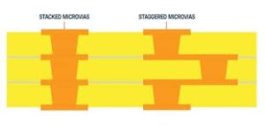
Conventional vias are round holes that run through the insulating layer of a printed circuit board (PCB). They’re drilled, filled with conductive material and plated with copper on both sides to make electrical connections between layers. stacked vias are like conventional vias, except they’re positioned closer together. Stacked vias are typically placed on the same layer of a PCB, and can be paired up to provide parallel or series connections.
How do you ensure quality control in stacked vias? Stacked vias require more precision than traditional vias. The tight tolerances of stacked vias can lead to misregistration during the PCB fabrication process. Misregistration is a common cause of poor quality in PCBs, and can result in higher rejection rates and increased costs. To counter this, manufacturers often use a technique called staggered vias to help mitigate the precision mandate of high aspect ratio stacked vias.
How Do You Ensure Quality Control in Stacked Vias?
The manufacturing process for a PCB involves several lamination cycles under high temperature and pressure. Each successive lamination cycle can reduce the accuracy of drilled microvias and cause them to drift from their design specifications. This can lead to failure during the final stages of assembly. Staggered vias can help prevent this type of error by ensuring that drilled holes in adjacent layers are not lined up directly with each other.
When a stacked via is drilled, the operator must place it on top of a blind or unfilled microvia that is already in place on the layer below. This can cause a void in the bottom of the hole and poor bonding between the base of the stacked via and the pad below it. This can lead to a lack of reliability, and may also impact signal transmission.
In a stacked via system, the plated copper on each layer is sandwiched between two narrow annular rings. These rings are designed to ensure the via has good structure, and to minimize stress at the interface between the plated metal and the copper in the surrounding area. When a stacked via experiences thermal cycling, the deposited copper can experience a stress fracture at the butt joint between the two rings. This can result in a lack of reliability and an increase in the failure rate for that particular stack up.
In addition to the reliability concerns of stacked vias, there are other issues that designers need to be aware of. For instance, a void in the copper plating of a stacked via can cause high-speed signals to carry noise from one side of the PCB to the other. This noise is known as crosstalk, and can cause poor performance. Staggered vias can help to mitigate this issue by offsetting the position of the vias between layers. This helps to isolate the noise, and minimizes the effect on high-speed signal integrity.


