
PCB Assembly and Manufacturing Compare to Traditional Wiring Harnesses
A printed circuit board (PCB) contains all of the components necessary to make an electronic device work. It can be used for a variety of purposes and functions, and it’s a great option for bringing innovative products to market in an efficient manner. However, PCB manufacturing and assembly can be a complicated process. Choosing the right build for your product requires careful consideration. Let’s take a look at how pcb assembly and manufacturing compare to traditional wiring harnesses.
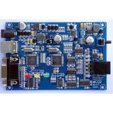
PCB assembly is a multistep process that starts with fabrication and ends with the finished product. It includes the assembly of small components onto a bare PCB, known as a printed circuit board assembly (PCBA). The PCBA process is used for mass-produced electronics because it is more cost-effective than other methods of creating a PCB, such as through-hole assembly.
In the fabrication process, a PCB’s blueprint is printed onto a piece of laminate material. After this, a layer of copper foil is added. The purpose of the copper is to allow electrical signals to travel between parts on the PCB, similar to how your nervous system carries messages from your brain to your muscles. The next step is to solder the traces of copper on the board. This is done through a process called reflow soldering, in which heat is applied to the circuit board to melt the solder and allow it to bond with the copper.
How Do PCB Assembly and Manufacturing Compare to Traditional Wiring Harnesses?
Once the solder has cooled, it is then inspected for flaws and imperfections by an automated machine known as an automatic optical inspection (AOI) machine. The AOI machine uses high-powered cameras to inspect each circuit board by looking at the light that reflects off of it. This is a quick and accurate way to identify any low-quality solder connections.
Once the reflow soldering and AOI inspection are complete, it’s time to add the components that will make up the final PCB. The most common method of doing this is through surface mount technology (SMT). This involves placing small, delicate components on the surface of the PCB, using a pick and place machine to do so. This type of machine can be used to mount components as small as a diode or a resistor.
Manual checks are also performed on each circuit board after the reflow soldering and aeration process. This can be a good alternative to automated AOI for smaller batches, but can quickly become impractical and inaccurate with larger quantities of boards. Looking at a PCB for hours can cause “optical fatigue,” which leads to decreased accuracy when inspecting for quality defects.
When comparing pcb assembly and manufacturing to traditional wiring harnesses, it’s important to consider all of the variables involved in the assembly process. The PCBA process is a complex procedure with many steps, and even a minor error can lead to costly errors that negatively impact production and product quality. However, when performed properly by an experienced and qualified team, the advantages of a PCBA are clear.

;Resize=(1180))
