

Impact of HDI PCB on Device Performance
With the escalating demand for smaller and lighter electronic devices, high-density interconnect (HDI) technology is an essential tool in the design process. This advanced technology enables manufacturers to pack a variety of 2.5-D and 3-D semiconductor packages into state-of-the-art electronics without compromising on performance. However, despite the impressive capabilities of HDI circuit boards, they are not without their own unique challenges and constraints. In this article, we will look at the key factors that can impact the performance of HDI PCBs and offer some best practices to help you overcome them.
Increased Connection Density: HDI PCBs provide increased connections per unit area by utilizing microvias, which are small holes with a diameter of less than 150 microns, drilled using a laser rather than through conventional mechanical drilling methods. They can be used to connect one layer to its adjacent layers and enable higher density, allowing designers to build more complex electronic products with the same footprint as older boards. This also improves signal integrity by reducing transmission delay and electromagnetic interference, which is particularly important in high-frequency applications.
Specialized Equipment: hdi pcb require specialized laser drilling machines, component placement systems, and inspection tools to achieve the tight tolerances required. This can add to the overall manufacturing cost.
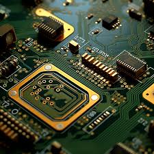
What is the Impact of HDI PCB on Device Performance?
Thermal Management: As the number of components on a HDI PCB increases, so does the heat generated, which must be effectively dissipated to avoid premature component failure and other problems. Improper thermal management can lead to elevated operating temperatures, which can degrade performance and cause reliability issues in the long run. To ensure proper thermal connectivity, it is essential to use a well-planned design and consider external cooling solutions if necessary.
Power Distribution: It is crucial to distribute the power efficiently throughout the board by ensuring adequate decoupling, minimizing voltage drops, and maintaining high-speed signal integrity in high-performance applications. This can be achieved by utilizing the power plane, grounding vias, and proper trace geometry.
Impedance Control: The close spacing of traces in HDI PCBs can create impedance discontinuities that reduce signal quality and may lead to crosstalk. This can be mitigated by utilizing proper impedance matching and controlled trace geometries to minimize unwanted reflections.
Choosing the right PCB stack-up is crucial to ensure that your device performs as intended. It is recommended to choose a lower-layer count, as boards with more layers will require more lamination and drilling cycles, leading to higher manufacturing costs. It is also advisable to optimize for single-sided layouts, as they will allow you to minimize the number of sequential layers and thereby reduce the number of drilling and lamination cycles. Finally, it is a good idea to minimize the number of plated through-holes (PTH) as much as possible, since they increase the cost and complexity of assembly, particularly in multi-layer boards. In addition, you should always minimize the amount of unused space on the surface of the PCB to reduce signal losses. This can be done by careful planning of fanouts for complex ICs and by optimizing the stack-up to take advantage of the maximum space available on the PCB.


